
Voltage controlled delay (AMORE)
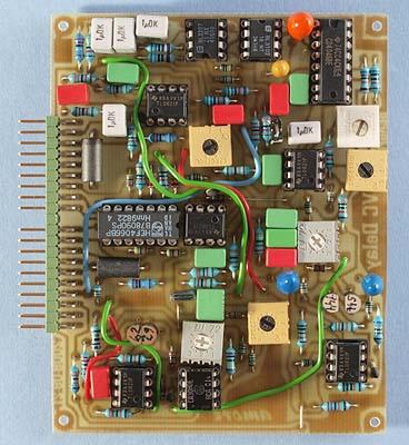
The final version of the board.
Delay isn't one of the
”classic” modular synth modules. Maybe this is because
analog delay chips became available when the synth industry had moved
on to non-modular and polyphonic synths.
This module is
based on the MN3207 BBD chip or it's modern equivalent, the BL3207.
The latter is still produced and can be had for a very modest sum of
money (you can buy it here).
This is a 1024 stage chip and the board should also work with the
2040 stage BL3208, if you want a longer delay. The board also uses
the companion clock chip MN3102/BL3102.
The delay time is voltage
controlled, by using the VCO part from a standard 4046 PLL chip. An
exponental converter controls the frequency of the PLL VCO. The delay
circuit and anti-aliasing filters is based on the MN3207 application
circuit from the datasheet.
I increased the cutoff of the anti-aliasing filter by dividing all
capacitor values with 1.5. Note that the BBD chip runs on +10 V
single supply, which is the maximum supply voltage. So for this
module, the +10 volt pin on the AMORE connector is used and therefore
you need the 10 volt supply that is specified in the standard, in
addition to +15 and -15 volts.
The board also contains a
3080-based VCA, which is used to give voltage control over the delay
feedback. There is a high pass filter that rolls off the bass in the
feedback loop. Otherwise the self-oscillation will occur at a very
low frequency (1/delay time), which isn't very musical. If you don't
want this bass roll-off, you can substiture the 15 nF capacitor with
a 1 µF one.
The feedback loop has external
connections so you could patch in other modules in the feedback loop
if you want. Note that there is a jumper on the board for completing
an internal feedback path (below/to the left of the 4046). This
jumper must be removed if you want to use an external feedback path.
The jumper can also be removed for troubleshooting. The CA3080 OTA
can be difficult to find nowadays but you can get it from Banzai
Effects, where you can get the BBD chips too.
This module should not be used if you just want delay, with the cleanest possible sound. For that, you should use a digital delay. The purpose of this module is to give coloration to the sound. This can be done by using varying amounts of feedback, to sum the delayed signal with the undelayed and/or to modulate the delay time. Note also that this module has limited bandwidth, so it will cut some treble. If you let this module self-oscillate while controlling it's parameters, you can get really weird and nasty sounds – but in a good way.
Bill of materials
You should have access
to the parts in the general bill of
materials.
In addition, you need the following less common
parts:
MN3207/BL3207
Bucket brigade delay IC
MN3102/BL3102 Clock IC
CD4046 PLL IC
Trimming
There are no less than six trimmers on this board:
Max freq, Min
freq
These sets the lowest and highest frequency of the clock.
Adjust these before you even plug the BBD chip into it's socket. The
maximum frequency should be trimmed to 400 kHz then the delay CV is
10 V. This is the maximum allowed clock frequency for the MN3207. You
could try to overclock it but I don't know if this might damage the
chip. The minimum frequency can be set according to taste, when the
delay CV is 0 V. Around 30 kHz if you want to avoid aliasing
completely or 20 kHz if you want to get more creative with the
sound.
BBD offset
Adjust
this while feeding the input a triangle wave at full amplitude. It
should be set so that the triangle clips symmetrically. If this
trimmer is unadjusted, there might not come any sound out of the
circuit.
VCA offset
Adjust
this with no input signal and the internal feedback jumper removed.
Measure the output of the VCA and adjust the trimmer so there is as
little DC change as possible when you sweep the feedback CV.
Fbk drive, Fbk
trim
The VCA used for feedback can be overdriven to compress
the signal. This helps to control self oscillation and shape the
sound. Adjust the trimmer ”Fbk drive” to taste. Then
adjust the trimmer ”Fbk trim” so that the circuit just
starts to self-oscillate when the feedback CV is full-on (10V).
Skill level required: LOW
There isn't really anything particularly difficult on this module. There is no real need to match transistors or other components. The board is a bit densely populated but as long as you get parts of the right size, this shouldn't cause problems.
|
Connector pin |
signal |
on this module |
|
1 |
1 oct/V |
not used |
|
2 |
in 1 |
main input |
|
3 |
CV 1 |
not used |
|
4 |
CV 2 |
not used |
|
5 |
CV 3 |
not used |
|
6 |
-15 V |
-15 V |
|
7 |
out 1 |
main output |
|
8 |
-1 V |
-1 V |
|
9 |
gnd |
gnd |
|
10 |
key |
- |
|
11 |
switch 1 |
bypass |
|
12 |
switch 2 |
mute |
|
13 |
out 2 |
VCA output |
|
14 |
+15 V |
+15 V |
|
15 |
+10 V |
+10 V |
|
16 |
aux output |
not used |
|
17 |
in 2 |
feedback input |
|
18 |
CV 4 |
feedback CV |
|
19 |
CV 5 |
delay CV |
|
20 |
CV 6 |
not used |